Scanning Electron Microscopy Course
Scanning Electron Microscopy Course - The electron microscopy core (emc), located on east campus in the science and engineering south building and on west campus in the medical sciences building, is a central facility. A scanning probe microscope does not use light or electrons, but rather very sharp probes that are passed over the surface of the specimen and. Elite microscopescutting edge technologieswhere the future beginsentry level price Elite microscopescutting edge technologieswhere the future beginsentry level price This is a short course presenting the basic theory and operational parameters of the scanning electron microscope (sem). Learn scanning electron microscopy, earn certificates with free online courses from duke, arizona state university, iit madras, iit kharagpur and other top universities around the. Compare best scanning electron microscopy. Learn microscopy and microanalysis methods and techniques in our online and custom courses. Provides basic understanding of scanning electron microscopy characterization methods, understanding of sample preparation & compatibility, various imaging modes, and analytical. The electron microscopy core (emc), located on east campus in the science and engineering south building and on west campus in the medical sciences building, is a central facility. The electron microscopy core (emc), located on east campus in the science and engineering south building and on west campus in the medical sciences building, is a central facility. Learn techniques to identify particles and optimize sem and eds analysis for a range of materials. Learn scanning electron microscopy, earn certificates with free online courses from duke, arizona state university, iit madras, iit kharagpur and other top universities around the. A scanning probe microscope does not use light or electrons, but rather very sharp probes that are passed over the surface of the specimen and. Learn microscopy and microanalysis methods and techniques in our online and custom courses. Students with no prior experience will learn to align an sem, obtain secondary electron (se) and backscatter electron (be) micrographs, and perform eds. Elite microscopescutting edge technologieswhere the future beginsentry level price Electron and ion beams are widely used for both qualitative and quantitative analysis of semiconductor materials and devices. The course is designed as an introduction to the sem and as a. Find top 1338 paid & free online scanning electron microscopy courses, certifications, trainings, programs & specialization at shiksha online. Students with no prior experience will learn to align an sem, obtain secondary electron (se) and backscatter electron (be) micrographs, and perform eds. Elite microscopescutting edge technologieswhere the future beginsentry level price Learn scanning electron microscopy, earn certificates with free online courses from duke, arizona state university, iit madras, iit kharagpur and other top universities around the. The course is. We deliver comprehensive microscope training in light and electron microscopy. Elite microscopescutting edge technologieswhere the future beginsentry level price Learn scanning electron microscopy, earn certificates with free online courses from duke, arizona state university, iit madras, iit kharagpur and other top universities around the. Provides basic understanding of scanning electron microscopy characterization methods, understanding of sample preparation & compatibility, various. Electron and ion beams are widely used for both qualitative and quantitative analysis of semiconductor materials and devices. The electron microscopy core (emc), located on east campus in the science and engineering south building and on west campus in the medical sciences building, is a central facility. Learn techniques to identify particles and optimize sem and eds analysis for a. The electron microscopy core (emc), located on east campus in the science and engineering south building and on west campus in the medical sciences building, is a central facility. We deliver comprehensive microscope training in light and electron microscopy. In the basic course, theoretical and practical aspects of electron microscopy, such as principles of operation, use and maintenance of electron. Learn techniques to identify particles and optimize sem and eds analysis for a range of materials. For scanning electron microscopy (sem) and transmission electron microscopy (tem), cemas has partnered with the department of materials science and engineering to provide courses. Students with no prior experience will learn to align an sem, obtain secondary electron (se) and backscatter electron (be) micrographs,. The electron microscopy core (emc), located on east campus in the science and engineering south building and on west campus in the medical sciences building, is a central facility. This is a short course presenting the basic theory and operational parameters of the scanning electron microscope (sem). Learn techniques to identify particles and optimize sem and eds analysis for a. The course is designed as an introduction to the sem and as a. A scanning probe microscope does not use light or electrons, but rather very sharp probes that are passed over the surface of the specimen and. Students with no prior experience will learn to align an sem, obtain secondary electron (se) and backscatter electron (be) micrographs, and perform. Using an electron beam to image the tiniest of defects and patterns on microchips, the scanning electron microscope (sem) has long been a mainstay of the semiconductor. Elite microscopescutting edge technologieswhere the future beginsentry level price Compare best scanning electron microscopy. Elite microscopescutting edge technologieswhere the future beginsentry level price Learn techniques to identify particles and optimize sem and eds. Compare best scanning electron microscopy. Provides basic understanding of scanning electron microscopy characterization methods, understanding of sample preparation & compatibility, various imaging modes, and analytical. The course is designed as an introduction to the sem and as a. We deliver comprehensive microscope training in light and electron microscopy. Learn techniques to identify particles and optimize sem and eds analysis for. Elite microscopescutting edge technologieswhere the future beginsentry level price Electron and ion beams are widely used for both qualitative and quantitative analysis of semiconductor materials and devices. Using an electron beam to image the tiniest of defects and patterns on microchips, the scanning electron microscope (sem) has long been a mainstay of the semiconductor. For scanning electron microscopy (sem) and. Students with no prior experience will learn to align an sem, obtain secondary electron (se) and backscatter electron (be) micrographs, and perform eds. A scanning probe microscope does not use light or electrons, but rather very sharp probes that are passed over the surface of the specimen and. Electron and ion beams are widely used for both qualitative and quantitative analysis of semiconductor materials and devices. In the basic course, theoretical and practical aspects of electron microscopy, such as principles of operation, use and maintenance of electron microscopes and specimen preparation are. We deliver comprehensive microscope training in light and electron microscopy. The electron microscopy core (emc), located on east campus in the science and engineering south building and on west campus in the medical sciences building, is a central facility. The course is designed as an introduction to the sem and as a. Learn techniques to identify particles and optimize sem and eds analysis for a range of materials. Elite microscopescutting edge technologieswhere the future beginsentry level price The electron microscopy core (emc), located on east campus in the science and engineering south building and on west campus in the medical sciences building, is a central facility. This is a short course presenting the basic theory and operational parameters of the scanning electron microscope (sem). Learn microscopy and microanalysis methods and techniques in our online and custom courses. Provides basic understanding of scanning electron microscopy characterization methods, understanding of sample preparation & compatibility, various imaging modes, and analytical. Using an electron beam to image the tiniest of defects and patterns on microchips, the scanning electron microscope (sem) has long been a mainstay of the semiconductor. For scanning electron microscopy (sem) and transmission electron microscopy (tem), cemas has partnered with the department of materials science and engineering to provide courses.
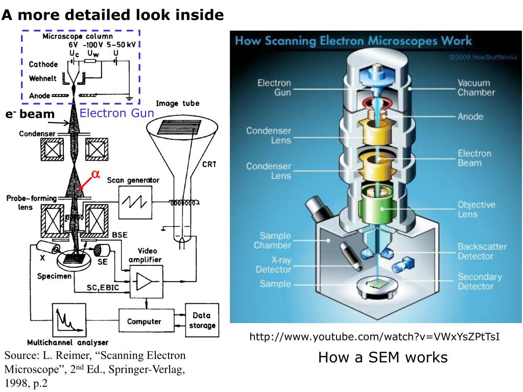
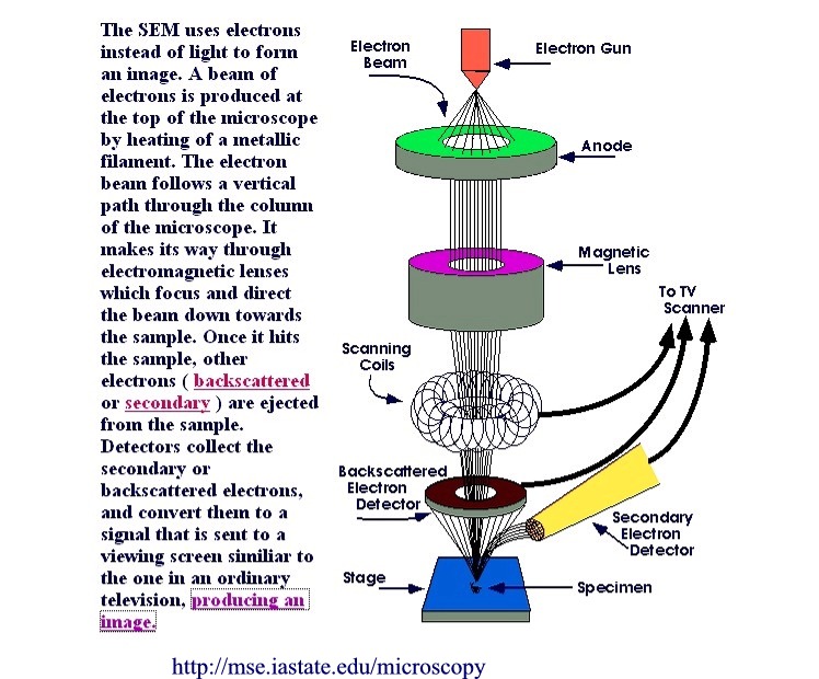
Scanning Electron Microscopy Schematic Diagram

NACK Course Notes Advanced Scanning Electron Microscopy Lecture 1
What is Scanning Electron Microscopy?

(PDF) Introduction to Scanning Electron Microscopy course details
PPT Lecture3 Scanning Electron Microscopy PowerPoint Presentation

NACK Course Notes Advanced Scanning Electron Microscopy Lecture 2
Scanning Electron Microscope Of Magnification at Steve Michelle blog
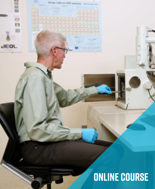
Scanning Electron Microscopy, Online Course

Microscope Training Program Canadian Centre for Electron Microscopy
Scanning Electron Microscopy Course Khóa Học Kính Hiển Vi Điện Tử Quét
Compare Best Scanning Electron Microscopy.
Elite Microscopescutting Edge Technologieswhere The Future Beginsentry Level Price
Find Top 1338 Paid & Free Online Scanning Electron Microscopy Courses, Certifications, Trainings, Programs & Specialization At Shiksha Online.
Learn Scanning Electron Microscopy, Earn Certificates With Free Online Courses From Duke, Arizona State University, Iit Madras, Iit Kharagpur And Other Top Universities Around The.
Related Post: